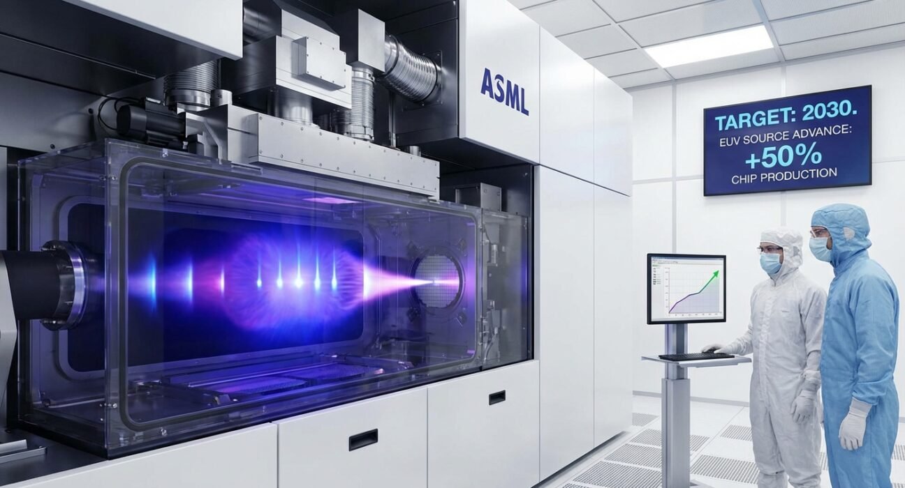
ASML, the Dutch semiconductor equipment giant, has revealed a significant technological breakthrough in its extreme ultraviolet (EUV) lithography systems that promises to drastically improve the speed and efficiency of global chip manufacturing. The company announced that it has successfully developed a way to increase the power of the light source in its machines, a move projected to boost chip production capacity by up to 50% by 2030.
The advancement centers on the laser-produced plasma source used in ASML‘s lithography scanners, which are the only machines in the world capable of printing the most advanced microchips. According to Michael Purvis, the company’s lead technologist for EUV light sources, researchers have successfully demonstrated a system capable of sustaining 1,000 watts (1 kilowatt) of EUV power. This represents a major leap from the current standard of approximately 600 watts used in high-volume manufacturing today.
Teun van Gogh, the Executive Vice President of ASML‘s NXE business line, confirmed that this power increase is directly tied to throughput. By the end of the decade, the company expects its machines to process around 330 silicon wafers per hour, compared to the roughly 220 wafers per hour achievable with current systems. This increase in productivity is critical for chipmakers like TSMC, Intel, and Samsung, as it allows them to produce more chips without needing to build as many expensive new factories or purchase as many additional machines.
The engineering behind this breakthrough involves optimizing the complex process of generating EUV light. In ASML‘s systems, light is created by firing high-powered carbon dioxide lasers at microscopic droplets of molten tin. To achieve the 1,000-watt milestone, engineers have doubled the frequency of these tin droplets to approximately 100,000 per second. Additionally, the system utilizes a refined laser-pulsing technique to shape the droplets more effectively before they are vaporized into plasma, thereby increasing the efficiency of the light generation.
This development comes at a crucial time for the semiconductor industry, which is facing insatiable demand for high-performance computing chips driven by the artificial intelligence boom. Reducing the “cost per wafer” is a primary goal for manufacturers, and ASML‘s upgrade addresses this by allowing existing and future fab footprints to yield significantly higher output. Purvis noted that the new system is “not a parlor trick” and has been tested to meet the rigorous operational requirements of commercial fabrication plants.
While ASML is also rolling out its newer High-NA EUV machines (the EXE series) for the next generation of 2-nanometer and smaller logic nodes, this light source upgrade appears to offer a performance extension for the widely used NXE platform as well. This ensures that the industry’s workhorse machines can continue to scale in productivity through the 2030 timeline.
The announcement reinforces ASML‘s absolute dominance in the lithography market. As the sole supplier of EUV technology, the company plays a linchpin role in the global tech supply chain. By pushing the physical limits of their light sources, ASML is effectively rewriting the economic roadmap for Moore’s Law, ensuring that the cost of computing power can continue to decline even as the complexity of manufacturing advanced semiconductors rises.